Introduction
In the 1990s, early NAND flash had latencies of over 1 millisecond and could only handle 10–20 MB/s read speeds. Write speeds were even worse, struggling at 5–10 MB/s.
But over the decades, advancements in controller technology, NAND cell design, and high-speed NVMe interfaces have driven massive improvements. Reliability has also improved with wear-leveling and error-correction algorithms.
Today’s NVMe SSDs achieve over 14,000 MB/s read and write speeds and latency as low as 10 microseconds—1000x faster than early flash.
In this article, we explore these dramatic transformations.
Note: For a look at how flash memory has evolved in capacity, cost, and form factor, check out our guide on the evolution of flash memory.
Sequential Read Speeds
It was in the mid-2000s—when the first SATA-based SSDs were introduced—that sequential read speeds underwent a significant improvement. The read speed at this time was in the range of several hundred megabytes per second. By 2010, modern SATA SSDs could reach read speeds of up to 500 MB/s. The next big breakthrough came with the introduction of NVMe SSDs around 2016. These SSDs used the PCIe interface and could deliver sequential read speeds of over 3 GB/s.
Key Milestones in the Evolution of Flash Memory – Sequential Read Speeds
| Year | Technology / Interface | Sequential Read Speed | Comments |
| 1990 | Early Flash Memory (Parallel) | 10–20 MB/s | Early NAND implementations (often experimental and lab-based) used simple parallel interfaces with basic cell designs that limited overall throughput. |
| 2002 | Early SSD Prototypes (IDE/SATA) | ~50–100 MB/s | Initial NAND-based SSDs began transitioning from parallel to serial interfaces; read speeds improved as controller algorithms started to manage NAND’s inherent latency. |
| 2006 | Early SATA SSD | 200–300 MB/s | Consumer NAND SSDs using SATA improved read speeds due to enhanced NAND cell fabrication and early error correction mechanisms that allowed for higher reliable throughput. |
| 2010 | Modern SATA SSD | ~500 MB/s | Advances in NAND flash density and controller design (including improved ECC and wear-leveling) enabled mainstream SATA SSDs to achieve stable, high read speeds. |
| 2016 | NVMe SSD (PCIe Gen 3) | 3,000+ MB/s | NVMe drives leveraged PCIe’s high bandwidth; NAND flash arrays benefitted from parallel data access and optimized command queues, significantly boosting sequential read speeds. |
| 2021 | NVMe SSD (PCIe Gen 4/5) | 5,000–15,000 MB/s | Latest NAND SSDs, utilizing PCIe Gen 4/5, further exploited advanced NAND architectures (e.g., high-density TLC/QLC with deep parallelism) for ultra-high read performance. |
Sequential Write Speeds
Early flash devices had a sequential write speed of only 5 to 10 MB/s. By the mid-2000s, SSDs began to achieve write speeds of around 150 to 300 MB/s. This improvement was due to the evolution of controller technologies and better error correction and caching methods. By 2010, modern SATA SSDs showed write speeds of around 450 MB/s. Around 2016, NVMe SSDs demonstrated write speeds in excess of 3 GB/s.
Key Milestones in the Evolution of Flash Memory – Sequential Write Speeds
| Year | Technology / Interface | Sequential Write Speed | Comments |
| 1990 | Early Flash Memory (Parallel) | 5–10 MB/s | Early NAND flash write operations were slow due to the necessity for block erase cycles and primitive programming algorithms that did not yet fully optimize NAND’s characteristics. |
| 2002 | Early SSD Prototypes (IDE/SATA) | ~50–100 MB/s | Early NAND SSD prototypes began using buffered writes and rudimentary wear leveling to improve throughput, though write speeds remained limited by NAND’s block-erase requirements. |
| 2006 | Early SATA SSD | 150–300 MB/s | Improvements in NAND cell architecture (e.g., better charge pump designs) and controller firmware enabled more efficient block writes, enhancing overall sequential write speeds. |
| 2010 | Modern SATA SSD | ~450 MB/s | Modern NAND SSDs using refined MLC designs and advanced controllers achieved higher write speeds while balancing wear-leveling and error correction overhead. |
| 2016 | NVMe SSD (PCIe Gen 3) | 3,000+ MB/s | NVMe SSDs harnessed the parallelism of NAND flash arrays and reduced command overhead to dramatically increase write speeds, even as advanced multi-bit per cell (TLC/QLC) designs became widespread. |
| 2021 | NVMe SSD (PCIe Gen 4/5) | 5,000–15,000 MB/s | Cutting-edge NAND technologies, including high-density TLC/QLC with aggressive parallelism and improved flash controllers, pushed write speeds higher while managing increased programming complexity. |
Latency
In early flash memory devices, latency was quite high—often around one to two milliseconds. By the time SSDs became mainstream, the latency had dropped to 0.5 milliseconds. This was around the mid-2000s. Later, SATA SSDs had a latency of about 0.1 milliseconds, and around 2016, NVMe SSDs were able to dramatically reduce the latency to 20 microseconds.
These reductions in latency have been instrumental in making flash memory the go-to memory choice for real-time computing applications.
Key Milestones in the Evolution of Flash Memory – Latency
| Year | Technology / Interface | Latency | Comments |
| 1990 | Early Flash Memory (Parallel) | 1–2 ms | Early NAND flash latency was high due to basic cell designs and inefficient control circuitry; individual cell access and block erasures added significant delay. |
| 2002 | Early SSD Prototypes (IDE/SATA) | ~0.8–1.0 ms | Transitioning to serial interfaces, early NAND SSDs began reducing latency with improved controllers, though still limited by legacy programming and erasure methods. |
| 2006 | Early SATA SSD | ~0.5 ms | Enhanced NAND flash chips with better process technology and improved firmware cut latency by streamlining the block management and error correction processes. |
| 2010 | Modern SATA SSD | ~0.1 ms | Continued advancements in NAND manufacturing and controller design reduced the overall access time; refined algorithms helped mitigate the inherent block-erase delay. |
| 2016 | NVMe SSD (PCIe Gen 3) | ~20 μs (0.02 ms) | NVMe’s optimized command queue, combined with NAND flash arrays managed in parallel, dramatically reduced latency by bypassing many legacy interface bottlenecks. |
| 2021 | NVMe SSD (PCIe Gen 4/5) | ~10 μs | Further refinements in NAND flash cell architecture and controller efficiency, alongside ultra-low latency protocols, brought average access times down to near-atomic levels. |
Endurance and Reliability
Reliability encompasses endurance, but it also refers to the overall ability of a flash memory device to maintain data integrity over time. It includes stable data retention, which is the capacity to hold charge without a power supply, low error rates during read and write operations, and resistance to temperature fluctuations and radiation.
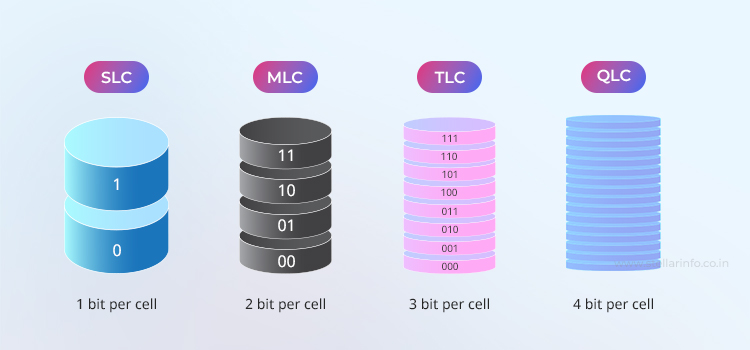
In the early days, Single-Level Cell (SLC) flash offered 100,000 to 1,000,000 P/E cycles. However, as manufacturers sought higher densities with Multi-Level Cell (MLC) technology, flash media with 2 or more bits per cell became the norm. But this came at a compromise, as MLC flash could offer an endurance of only about 5,000 to 10,000 cycles. Later, Triple-Level Cell (TLC) and Quad-Level Cell (QLC) technologies increased capacity but lowered the endurance to around 1,000 cycles (for TLC).
Key Milestones in the Evolution of Flash Memory – Reliability & Endurance
| Year | Flash Type | Typical Endurance (P/E Cycles) | Notes |
| Early 1990s | SLC | 100,000–1,000,000 | High endurance, simple design |
| Late 1990s / early 2000s | MLC | 5,000–10,000 | Increased density, reduced endurance |
| 2000s | TLC | ~1,000 | Higher bits per cell, lower endurance |
| Recent | 3D MLC / TLC | 1,500–40,000 (varies by design) | Enhanced by advanced controllers |
What's Next in Flash Technology?
Manufacturers are already exploring chips with 160 layers and beyond. However, as cell sizes become smaller and more bits are stored in each cell using MLC technology, reduced endurance and increased error rates become more pronounced.
To address these challenges, there is ongoing innovation in ECC methods and wear leveling. Additionally, techniques such as on-chip thermal annealing and self-healing are being researched.
Conclusion
For those interested in storage technology beyond flash, hard drives remain a critical option due to their cost-effective, high-capacity solutions. To explore how HDDs have improved over the past seven decades, check out our guides on the Evolution of Hard Disk Drives and the Key Specifications to Consider Before Buying a Hard Drive.


About The Author

Data Recovery Expert & Content Strategist